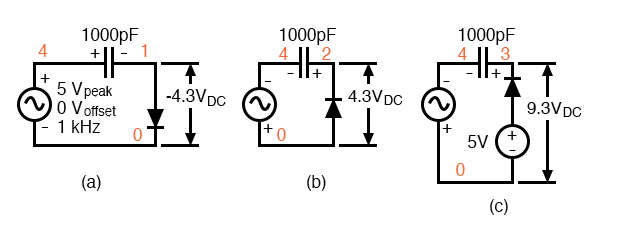
The circuits in the figure below are known as clampers or DC restorers. The corresponding netlist is also in the figure below. These circuits clamp a peak of a waveform to a specific DC level compared with a capacitively coupled signal which swings about its average DC level (usually 0V). If the diode is removed from the clamper, it defaults to a simple coupling capacitor– no clamping.
What is Clamp Voltage?
What is clamp voltage? And, which peak gets clamped? In the figure below (a) the clamp voltage is 0 V ignoring diode drop, (more exactly 0.7 V with Si diode drop).
Clamper Circuit Operation Analysis
In the figure below, the positive peak of V(1) is clamped to the 0 V (0.7 V) clamp level. Why is this? On the first positive half cycle, the diode conducts charging the capacitor left end to +5 V (4.3 V). This is -5 V (-4.3 V) on the right end at V(1,4).
Note the polarity marked on the capacitor in figure (a) below. The right end of the capacitor is -5 V DC (-4.3 V) with respect to ground. It also has an AC 5 V peak sine wave coupled across it from source V(4) to node 1. The sum of the two is a 5 V peak sine riding on a – 5 V DC (-4.3 V) level. The diode only conducts on successive positive excursions of source V(4) if the peak V(4) exceeds the charge on the capacitor. This only happens if the charge on the capacitor drained off due to a load, not shown. The charge on the capacitor is equal to the positive peak of V(4) (less 0.7 diode drop). The AC riding on the negative end, right end, is shifted down. The positive peak of the waveform is clamped to 0 V (0.7 V) because the diode conducts on the positive peak .

Clampers: (a) Positive peak clamped to 0 V. (b) Negative peak clamped to 0 V. (c) Negative peak clamped to 5 V.
|
|
*SPICE 03443.eps V1 6 0 5 D1 6 3 diode C1 4 3 1000p D2 0 2 diode C2 4 2 1000p C3 4 1 1000p D3 1 0 diode V2 4 0 SIN(0 5 1k) .model diode d .tran 0.01m 5m .end |
V(4) source voltage 5 V peak used in all clampers. V(1) clamper output from the Figure above (a). V(1,4) DC voltage on capacitor in Figure (a). V(2) clamper output from Figure (b). V(3) clamper output from Figure (c).
Suppose the polarity of the diode is reversed as in figure (b) above? The diode conducts on the negative peak of source V(4). The negative peak is clamped to 0 V (-0.7 V). See V(2) in the figure above.
The most general realization of the clamper is shown in figure (c) above with the diode connected to a DC reference. The capacitor still charges during the negative peak of the source. Note that the polarities of the AC source and the DC reference are series aiding. Thus, the capacitor charges to the sum to the two, 10 V DC (9.3 V). Coupling the 5 V peak sine wave across the capacitor yields the Figure above V(3), the sum of the charge on the capacitor and the sinewave. The negative peak appears to be clamped to 5 V DC (4.3V), the value of the DC clamp reference (less diode drop).
Describe the waveform if the DC clamp reference is changed from 5 V to 10 V. The clamped waveform will shift up. The negative peak will be clamped to 10 V (9.3). Suppose that the amplitude of the sine wave source is increased from 5 V to 7 V? The negative peak clamp level will remain unchanged. Though, the amplitude of the sinewave output will increase.
Clamper Circuits as DC Restorers
An application of the clamper circuit is as a “DC restorer” in “composite video” circuitry in both television transmitters and receivers. An NTSC (US video standard) video signal “white level” corresponds to a minimum (12.5%) transmitted power. The video “black level” corresponds to a high level (75% of transmitter power. There is a “blacker than black level” corresponding to 100% transmitted power assigned to synchronization signals. The NTSC signal contains both video and synchronization pulses.
The problem with the composite video is that its average DC level varies with the scene, dark vs light. The video itself is supposed to vary. However, the sync must always peak at 100%. To prevent the sync signals from drifting with changing scenes, a “DC restorer” clamps the top of the sync pulses to a voltage corresponding to 100% transmitter modulation. [ATCO]
REVIEW:
- A capacitively coupled signal alternates about its average DC level (0 V).
- The signal out of a clamper appears the have one peak clamped to a DC voltage. Example: The negative peak is clamped to 0 VDC, the waveform appears to be shifted upward. The polarity of the diode determines which peak is clamped.
- An application of a clamper, or DC restorer, is in clamping the sync pulses of composite video to a voltage corresponding to 100% of transmitter power.

