
Varicap or varactor diodes
A variable capacitance diode is known as a varicap diode or as a varactor. If a diode is reverse biased, an insulating depletion region forms between the two semiconductive layers. In many diodes the width of the depletion region may be changed by varying the reverse bias. This varies the capacitance. This effect is accentuated in varicap diodes. The schematic symbols is shown in the figure below, one of which is packaged as common cathode dual diode.
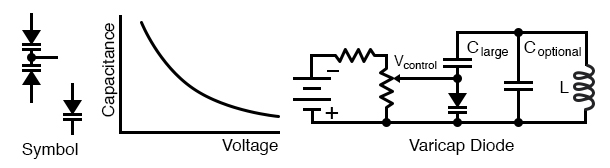
Varicap diode: Capacitance varies with reverse bias. This varies the frequency of a resonant network.
If a varicap diode is part of a resonant circuit as in the figure above, the frequency may be varied with a control voltage, Vcontrol. A large capacitance, low Xc, in series with the varicap prevents Vcontrol from being shorted out by inductor L. As long as the series capacitor is large, it has minimal effect on the frequency of resonant circuit. Coptional may be used to set the center resonant frequency. Vcontrol can then vary the frequency about this point. Note that the required active circuitry to make the resonant network oscillate is not shown. For an example of a varicap diode tuned AM radio receiver see “electronic varicap diode tuning,” Ch 9
Some varicap diodes may be referred to as abrupt, hyperabrupt, or super hyper abrupt. These refer to the change in junction capacitance with changing reverse bias as being abrupt or hyper-abrupt, or super hyperabrupt. These diodes offer a relatively large change in capacitance. This is useful when oscillators or filters are swept over a large frequency range. Varying the bias of abrupt varicaps over the rated limits, changes capacitance by a 4:1 ratio, hyperabrupt by 10:1, super hyperabrupt by 20:1.
Varactor diodes may be used in frequency multiplier circuits. See “Practical analog semiconductor circuits,” Varactor multiplier
Snap diode
The snap diode, also known as the step recovery diode is designed for use in high ratio frequency multipliers up to 20 gHz. When the diode is forward biased, charge is stored in the PN junction. This charge is drawn out as the diode is reverse biased. The diode looks like a low impedance current source during forward bias. When reverse bias is applied it still looks like a low impedance source until all the charge is withdrawn. It then “snaps” to a high impedance state causing a voltage impulse, rich in harmonics. An applications is a comb generator, a generator of many harmonics. Moderate power 2x and 4x multipliers are another application.
PIN diodes
A PIN diode is a fast low capacitance switching diode. Do not confuse a PIN switching diode with a PIN photodiode. A PIN diode is manufactured like a silicon switching diode with an intrinsic region added between the PN junction layers. This yields a thicker depletion region, the insulating layer at the junction of a reverse biased diode. This results in lower capacitance than a reverse biased switching diode.
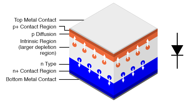
Pin diode: Cross section aligned with schematic symbol.
PIN diodes are used in place of switching diodes in radio frequency (RF) applications, for example, a T/R switch. The 1n4007 1000 V, 1 A general purpose power diode is reported to be usable as a PIN switching diode. The high voltage rating of this diode is achieved by the inclusion of an intrinsic layer dividing the PN junction. This intrinsic layer makes the 1n4007 a PIN diode. Another PIN diode application is as the antenna switch here for a direction finder receiver.
PIN diodes serve as variable resistors when the forward bias is varied. One such application is the voltage variable attenuator. The low capacitance characteristic of PIN diodes, extends the frequency flat response of the attenuator to microwave frequencies.
IMPATT diode
IMPact Avalanche Transit Time diode is a high power radio frequency (RF) generator operating from 3 to 100 gHz. IMPATT diodes are fabricated from silicon, gallium arsenide, or silicon carbide.
An IMPATT diode is reverse biased above the breakdown voltage. The high doping levels produce a thin depletion region. The resulting high electric field rapidly accelerates carriers which free other carriers in collisions with the crystal lattice. Holes are swept into the P+ region. Electrons drift toward the N regions. The cascading effect creates an avalanche current which increases even as voltage across the junction decreases. The pulses of current lag the voltage peak across the junction. A “negative resistance” effect in conjunction with a resonant circuit produces oscillations at high power levels (high for semiconductors).
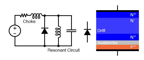
IMPATT diode: Oscillator circuit and heavily doped P and N layers.
The resonant circuit in the schematic diagram of the figure above is the lumped circuit equivalent of a waveguide section, where the IMPATT diode is mounted. DC reverse bias is applied through a choke which keeps RF from being lost in the bias supply. This may be a section of waveguide known as a bias Tee. Low power RADAR transmitters may use an IMPATT diode as a power source. They are too noisy for use in the receiver. [YMCW]
Gunn diode
Diode, gunn Gunn diode
A gunn diode is solely composed of N-type semiconductor. As such, it is not a true diode. The figure below shows a lightly doped N- layer surrounded by heavily doped N+ layers. A voltage applied across the N-type gallium arsenide gunn diode creates a strong electric field across the lightly doped N- layer.
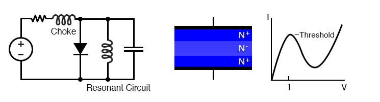
Gunn diode: Oscillator circuit and cross section of only N-type semiconductor diode.
As voltage is increased, conduction increases due to electrons in a low energy conduction band. As voltage is increased beyond the threshold of approximately 1 V, electrons move from the lower conduction band to the higher energy conduction band where they no longer contribute to conduction. In other words, as voltage increases, current decreases, a negative resistance condition. The oscillation frequency is determined by the transit time of the conduction electrons, which is inversely related to the thickness of the N- layer.
The frequency may be controlled to some extent by embedding the gunn diode into a resonant circuit. The lumped circuit equivalent shown in Figure above is actually a coaxial transmission line or waveguide. Gallium arsenide gunn diodes are available for operation from 10 to 200 gHz at 5 to 65 mw power. Gunn diodes may also serve as amplifiers. [CHW] [IAP]
Shockley diode
The Shockley diode is a 4-layer thyristor used to trigger larger thyristors. It only conducts in one direction when triggered by a voltage exceeding the breakover voltage, about 20 V. See “Thyristors,” The Shockley Diode. The bidirectional version is called a diac. See “Thyristors,” The DIAC.
Constant-current diodes
A constant-current diode, also known as a current-limiting diode, or current-regulating diode, does exactly what its name implies: it regulates current through it to some maximum level. The constant current diode is a two terminal version of a JFET. If we try to force more current through a constant-current diode than its current-regulation point, it simply “fights back” by dropping more voltage. If we were to build the circuit in figure(a) below(a) and plot diode current against diode voltage, we’d get a graph that rises at first and then levels off at the current regulation point as in figure(b) below(b).
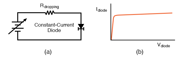
Constant current diode: (a) Test circuit, (b) current vs voltage characteristic.
One application for a constant-current diode is to automatically limit current through an LED or laser diode over a wide range of power supply voltages as in the figure below.
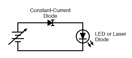
Constant current diode application: driving laser diode.
Of course, the constant-current diode’s regulation point should be chosen to match the LED or laser diode’s optimum forward current. This is especially important for the laser diode, not so much for the LED, as regular LEDs tend to be more tolerant of forward current variations.
SiC diodes
Diodes manufactured from silicon carbide are capable of high temperature operation to 400 °C. This could be in a high temperature environment: down hole oil well logging, gas turbine engines, auto engines. Or, operation in a moderate environment at high power dissipation. Nuclear and space applications are promising as SiC is 100 times more resistant to radiation compared with silicon. SiC is a better conductor of heat than any metal. Thus, SiC is better than silicon at conducting away heat. Breakdown voltage is several kV. SiC power devices are expected to reduce electrical energy losses in the power industry by a factor of 100.
Polymer diode
Diodes based on organic chemicals have been produced using low temperature processes. Hole rich and electron rich conductive polymers may be inkjet printed in layers. Most of the research and development is of the organic LED (OLED). However, development of inexpensive printable organic RFID (radio frequency identification) tags is on going. In this effort, a pentacene organic rectifier has been operated at 50 MHz. Rectification to 800 MHz is a development goal. An inexpensive metal insulator metal(MIM) diode acting like a back-to-back zener diode clipper has been developed. Also, a tunnel diode like device has been fabricated.